


Services on Demand
Journal

Article
 Article in xml format
 Article references
 Send this article by e-mail
Indicators
-
 Cited by SciELO
Related links
-
 Similars in
SciELO
Similars in
SciELO
Share

 Permalink
Anales de la Asociación Química Argentina
Print version ISSN 0365-0375
An. Asoc. Quím. Argent. vol.93 no.1-3 Buenos Aires Jan./July 2005
ELECTRONIC NOSES APPLICATIONS AND TECHNOLOGIES
Monitoring of state of charge in MOS capacitors by pulsed photocurrentLombardi, R.; Aragón, R.*
Laboratorio de Películas Delgadas, Facultad de Ingeniería, Universidad de Buenos Aires, Paseo Colón 850 C.P. 1063, Buenos Aires, Argentina
*CINSO-CONICET-CITEFA. Lasalle 4397, Villa Martelli, Buenos Aires, Argentina.
Fax: (54) 11 4331 0129, E-mail:raragon@fi.uba.ar
Received November 05, 2004. In final form March 28, 2005
Abstract
Pulsed illumination of a biased MOS capacitor through windowed gates induces a photocurrent which can be used to monitor shifts of bias voltage, in response to a gaseous chemical stimulus. If collimation requirements are relaxed, to allow the use of comparatively simple LED light sources, increased window area must be adopted to compensate for the reduced light intensity. Experimental and modelled responses demonstrate that useful information may still be obtained, limited by the convolution of response with a finite beam diameter and constrained by window size.
Resumen
Iluminación pulsada sobre un capacitor MOS polarizado, a través de una compuerta con ventana induce una fotocorriente, que puede usarse para monitorear los corrimientos en polarización, en respuesta a un estímulo químico gaseoso. Si los requerimientos de colimación se relajan, para permitir el uso de fuentes de luz comparativamente simples, deben adoptarse ventanas de mayor área para compensar la reducción de la intensidad del haz. Tanto las respuestas experimentales como modeladas demuestran que puede aun obtenerse información útil, limitada por la convolución de la respuesta con el haz de diámetro finito y por el tamaño de la ventana.
Introduction
The photocurrent induced by pulsed illumination of a MOS structure, through biased light transmitting gates, has been shown [1] to be a sensitive probe of capacitor charge state, capable of detecting bias shifts in response to a chemical stimulus, and subsequent investigations [2] have demonstrated that discontinuous gates, unimpaired by electrode light absorption, provide even higher sensitivity.
With the use of windowed gates, light intensity requirements are reduced to the point that simple LED sources can substitute for the highly collimated laser beams employed in SPLT (Scanned Pulsed Laser Technique), if the lower fluxes are compensated by the increased window area. This study surveys the limits of application of macroscopic beams on windowed gate MOS devices.
Experimental
100 nm thick palladium gates, with 2.5 mm circular windows, were magnetron sputtered through shadow masks, onto p-type (100) silicon wafers, thermally oxidised to 130 nm. Light from a current controlled, low divergence (+/- 3°), 630 nm wavelength, light emitting diodes, TTL pulsed at fixed frequency (1, 10 and 100 kHz) was piped into the window centre, through a 1.75 mm core optic fiber and the photocurrent monitored, after I/V conversion (104 V/A), with a Signal Recovery DSP 7265 lock-in amplifier, as a function of DC bias voltage.
Model equivalent circuit and response
The equivalent circuit (Fig. 1) for a MOS capacitor under pulsed illumination [1] of intensity F0 allocates dc induced minority carrier photocurrent ig, to bulk (ibr) and surface (isr) recombination processes, in addition to the displacement current ( id), converted to a measurable voltage (u) by the load resistor (RL), which can be described by:

where: s represents the surface recombination rate; ys, the Si surface potential; Dn the carrier diffusion coefficient; Ln the Debye length; k, Boltzmann’s constant; T, the absolute temperature and x0 , the cut-off width for the channel at the Si-SiO2 interface.
The associated potential V is the sum of three contributions, namely:
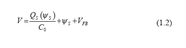
where: VFB is the flat band voltage, and the surface charge Qs corresponds to [3]:
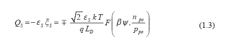
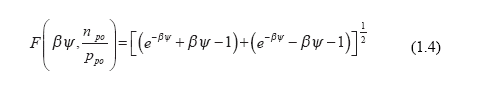
in which the adimensional potential F responds to:
and the differential capacity CD is the derivative of Qs with respect to ys.
Invoking a lateral current flow model [4], Filippini and Lundström [2] evaluated the one dimensional potential, across the electrode gap defined by the gate window, as:
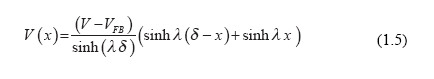
where: ![]() and the product cr is [5]:
and the product cr is [5]:
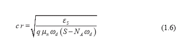
with: es, the Si permitivity; mn, the electron mobility in Si; wd, the depletion zone width [6] and NA, the acceptor concentration.

Fig. 1. Model equivalent circuit for a MOS capacitor under pulsed illumination.
Equation (1.5) can be solved to obtain the potential V(x) as a function of position and bias voltage (Fig. 2), which when substituted into Eq. (1.2), together with Eq.(1.3) and Eq.(1.4), for realistic physical or fitted parameters, permits numerical evaluation of ys (Fig. 3), and consequently of the response u, in Eq. (1.1)(Fig. 4).
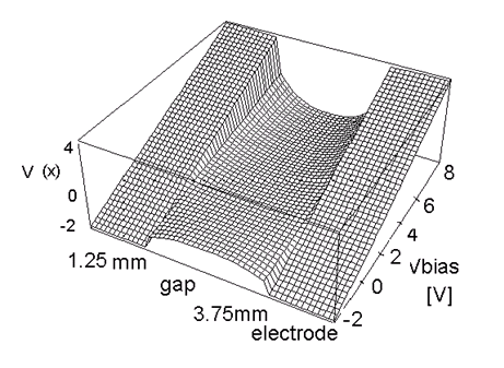
Fig. 2. One dimensional potential V, as a function of position across a windowed MOS capacitor with a 2.5 mm gap and dc bias voltage.
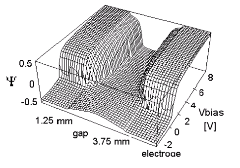
Fig. 3. Si Surface Potential (y), as a function of position across a windowed MOS capacitor with a 2.5 mm gap and dc bias voltage.
Fig. 4. Photocurrent response (u) in arbitrary units, as a function of position across a windowed MOS capacitor with a 2.5 mm gap and dc bias voltage.
Results and discussion
The effect of a finite beam width and the intensity distribution is accountable by the convolution (Fig. 5) of a Gaussian profile, radially distributed over a circle of fixed diameter, with the modelled response of Fig. 4. For a 1 mm beam diameter (Fig 5, a), a clear concentration of the response on the edges of the gap is still distinguishable, surrounding a dead zone of minimum signal centred in the gap. Substantial rounding of the almost unit step behaviour of u with bias voltage is present even at maximum signal strength but saturation occurs under deep inversion conditions. Increasing beam diameter to 2 mm (Fig 5, b) attenuates the features of the functional dependence with further smoothing, until, for beams in excess of the window diameter (Fig.5, c), all evidence of the dead zone is lost and the signal does not saturate at any potential. Increased operating frequency enhances these effects, because of its narrowing effect on the maximum response area width, due to increased l parameters (cf. Eqs. 1.5 and 1.6).
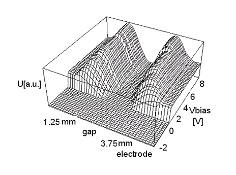
Fig. 5a. Convoluted photocurrent response (u) for 1mm beam diameter.

Fig. 5b. Convoluted photocurrent response (u), for 2mm beam diameter.
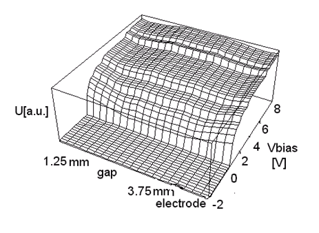
Fig. 5c.Convoluted photocurrent response (u), for 3mm beam diameter.
Comparison of the experimental dependence of u on bias voltage, for beam diameters between 1.8 and 2.3 mm at 1, 10 and 100 kHz (Fig 6 a, b, c) are in full agreement with the modelled response predictions.
Overall, signal decreases with increasing beam diameter, due to decreasing light flux density, and with increasing frequency, which is proportional to l . At 1.8 mm O.D., the centered beam spans the dead zone, whereas, at 2.0mm O.D., the signal strength increases despite lower illumination, because the active region near the electrodes is stimulated. Saturation is apparent only for the broadest beams and lower frequencies.
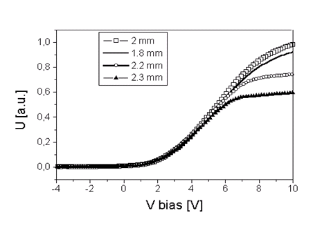
Fig. 6a. Measured photocurrent response (u) , as a function of bias voltage and beam size, at 1Khz.
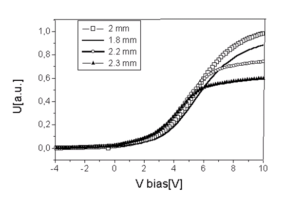
Fig. 6b. Measured photocurrent response (u) , as a function of bias voltage and beam size, at 10 Khz.
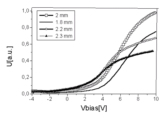
Fig. 6c. Measured photocurrent response (u) , as a function of bias voltage and beam size, at 100 Khz
Conclusions
The sensitivity of bias shift detection, in response to a chemical stimulus is proportional to the derivative of u with respect to bias voltage. The sharp sigmoidal characteristic of MOS devices is attenuated by convolution with broad beams, if wide gaps are used to compensate for lower illumination flux, because the principal contribution to the photocurrent originates from the immediate vicinity of the gate window edge.
For nondegenerate silicon wafers, the reduced response area can be eliminated for window diameters below 1mm. Increased pulsing frequency narrows the active area thus reducing overall signal strength.
References
[1] Engstrom, O.; Carlsson, A., J. Appl. Phys. 1983, 54, 5245. [ Links ]
[2] Filippini, D.; Lundström, I. J.Appl. Phys. 2002, 91, 3896. [ Links ]
[3] Sze, S. M. “Physics of Semiconductor Devices”, J. Wiley and Son, New York, 1981 [ Links ]
[4] Nicollian, E. H.; Goetzberger, A. IEEE Transactions on Electron Devices, 1965, 12, 108. [ Links ]
[5] Holmberg, M; Lundström, I. Appl Surf. Science, 1996, 93, 67. [ Links ]
[6] Muller, R.; Kamins, T. “Device Electronic for Integrated Circuits”, 2nd ed., J.Wiley and Sons, 1986. [ Links ]

