


Servicios Personalizados
Revista

Articulo
 Inglés (pdf)
 Articulo en XML
 Referencias del artículo
 Enviar articulo por email
Indicadores
-
 Citado por SciELO
Links relacionados
-
 Similares en
SciELO
Similares en
SciELO
Compartir

 Permalink
Papers in physics
versión On-line ISSN 1852-4249
Pap. Phys. vol.11 no.1 La Plata jun. 2019
On the impact of the stress situation on the optical properties of WSe2monolayers under high pressure
A. Francisco-Lopez,1 2 B. Han,3 4 D. Lagarde,3 X. Marie,3 B. Urbaszek,3 C. Robert,3 A. R. Goni1,3*
1*E-mail: goni@icmab.es
2Institut de Ciencia de Materials de Barcelona (ICMAB-CSIC), Campus de la UAB, 08193 Bellaterra, Spain.
3Universite de Toulouse, INSA-CNRS-UPS, LPCNO, 135 Avenue de Rangueil, 31077 Toulouse, France.
4ICREA, Passeig Lluís Companys 23, 08010 Barcelona, Spain.
Abstract
We have studied the optical properties of WSe2 monolayers (ML) by means of photolu-minescence (PL), PL excitation (PLE) and Raman scattering spectroscopy at room temperature and as a function of hydrostatic pressure up to ca. 12 GPa. For comparison, the study comprises two cases: A single WSe2 ML directly transferred onto one of the diamonds of the diamond anvil cell and a WSe2 ML encapsulated into hexagonal boron nitride (hBN) layers. The pressure dependence of the A and B exciton, as determined by PL and PLE, respectively, is very different for the case of the bare WSe2 ML and the hBN/WSe2-ML/hBN heterostructure. Whereas for the latter the A and B exciton energy increases linearly with increasing pressure at a rate of 3.5 to 3.8 meV/GPa, for the bare WSe2 ML the A and B exciton energy decreases with a coefficient of -3.1 and -1.3 meV/GPa, respectively. We interpret that this behavior is due to a different stress situation. For a single ML the stress tensor is essentially uniaxial with the compressive stress component in the direction perpendicular to the plane of the ML. In contrast, for the substantially thicker hBN/WSe2-ML/hBN heterostructure, the compression is hydrostatic. The results from an analysis of the pressure dependence of the frequency of Raman active modes comply with the interpretation of having a different stress situation in each case.
Keywords: dichalcogeneides, monolayers, high pressure, Raman, photoluminescence, stress-strain tensors
I. Introduction
Monolayers (MLs) of group-VI transition metal dichalcogenides (TMDs), MX2 with M=Mo, W and X= S, Se, Te, have emerged as fascinating two-dimensional (2D) semiconductors due to remark-able properties that differ from the bulk. For example, MLs possess a direct band gap located at the K points of the hexagonal Brillouin zone 1, 2. Electron-hole pairs are also strongly bound by Coulomb interactions giving rise to robust excitons with binding energies of several hundreds of meV 3. Due to the lack of inversion symmetry in the ML, both spin and K valley degrees of free-dom can be controlled using chiral optical selection rules 4. Finally, the strong spin-orbit coupling is responsible for large splittings in both valence and conduction band with several hundreds and tens of meV at the K points, respectively. This gives rise to a large variety of optically bright and dark excitons, governing the optical properties from cryogenic to room temperature. Bright excitons involving the first valence band are called A excitons, whereas those involving the second valence band are called B excitons. Dark excitons can be optically inactive due to several reasons. The most studied ones are the spin-forbidden dark excitons which have been identified experimentally in WSe2 and WS2 5-9. Momentum mismatch (indirect) excitons composed of electron and hole residing in different K valleys have also been predicted but a clear experimental identification is still lacking. Band structure calculations within density functional theory (DFT) have shown that conduction band minima at the Q points can be a few tens of meV above the K valleys in tungsten-based MLs 10. Because the effective mass at the Q points is expected to be larger than that at the K points, an indirect exciton composed of an electron in a Q valley and a hole in a K valley may have larger binding energy than a direct bright exciton with electron and hole both residing in the K valley. These indirect excitons may give rise to photoluminescence (PL) emission through phonon assisted process as suggested in Ref. 11.
High pressure methods combined with optical spectroscopy have demonstrated to be a powerful tool to tune the band structure and optical properties of semiconductors in general 13. Because the bands at different points of the Brillouin zone shift in energy with different pressure coefficients, high pressure experiments can be used to distinguish between k-space direct and indirect transitions. As far as truly two-dimensional (2D) TMD materials are concerned, there are already several reports on the dependence on hydrostatic pressure of the emission and vibrational properties of monolayers of MoS2 14-18, WSe2 19 and WS2 20. The results, however, are surprisingly contradictory. All studies were performed on MLs transferred or deposited on SiO2/Si wafers, except for the work of Ref. 20, in which authors also looked at the pressure behavior of the ML directly on the diamond anvil surface. We conducted high-pressure optical-spectroscopy experiments on WSe2 MLs on the diamond anvil and encapsulated by hBN layers for comparison. The encapsulation of TMD MLs using hexagonal boron nitride (hBN) layers contributes much to the preservation of the physical properties of the ML. In fact, narrower PL linewidths have been reported for hBN encapsulated MLs. In this work, we show that different stress situations hold in the two samples, being fully hydrostatic for the hBN/WSe2-ML/hBN heterostructure but uniaxial for the bare ML. This has direct impact on sign and magnitude of the pressure coefficient of the A and B excitons, for example.
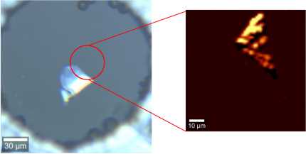
Figure 1: (Left panel) Optical image of the DAC loaded with a single-layer of WSe2 (plus some bulk and few layers) at a pressure of ca. 5.4 GPa. The monolayer is only apparent in the PL map (right panel), corresponding to a scan of the A-exciton peak intensity of the WSe2 ML across the sample.
II. Experimental details
For the high pressure experiments, the samples are mechanically exfoliated onto the surface of one of the diamond anvils of the high pressure cell (DAC). We thus transferred onto the diamond surface using a polydimethylsiloxane (PDMS) stamp either a WSe2 flake containing some bulk and few-layers parts as well as the desired single monolayer or a hBN/ML/hBN van der Waals (vdW) heterostruc-ture. The latter were fabricated by mechanical ex-foliation of bulk WSe2 (commercially available) and hBN crystals 21. A first layer of hBN is mechanically exfoliated onto a freshly cleaned diamond. The deposition of the subsequent WSe2 ML and the second hBN capping layer is obtained by re-peating this procedure. The left panel of Fig. 1 illustrates the result of loading the DAC with bare ML sample.
The high-pressure photoluminescence and micro-Raman scattering measurements were performed at room temperature employing a gasketed diamond anvil cell. A 4:1 methanol/ethanol mixture was used as pressure transmitting medium and a ruby sphere for pressure calibration 22. The photoluminescence (PL) spectra were excited with the 488 nm line of an Ar+-ion laser, whereas for the Raman measurements an infrared diode laser emit-ting at 785 nm was employed in addition to the 488 nm line. Spectra were collected using a 20x long working distance objective with NA=0.35 and dis-persed with a high-resolution LabRam HR800 grat-ing spectrometer equipped with a charge-coupled device detector. PL spectra were corrected for the spectral response of the spectrometer by normal-izing each spectrum using the detector and the 600-grooves/mm grating characteristics. The experiments were always performed illuminating the same spot on the sample by using reference marks within the field of view of our confocal microscope. PL maps of the samples loaded into the DAC were measured using a 633 nm HeNe laser in a WITec alpha 300 RA+ confocal setup and the same 20 x objective. The acquisition time was set to 100 ms per point and the PL images typically consisted of 100 x 100 pm2 regions analyzed in lateral steps of 2 pm (see right panel of Fig. 1). For PL ex-citation measurements (PLE) we used a Fianium SC-400-4 supercontinuum laser, tunable from 410 nm to 1000 nm. PL spectra in the spectral region of the ML maximum emission were measured with the LabRam HR800 spectrometer while the white laser was tuned in steps of 2 nm in the range from 450 to ca. 700 nm.
III. Results and discussion
i. PL and PLE under pressure
Figures 2a and 2b show several PL spectra of the bare WSe2 ML and the hBN/WSe2-ML/hBN vdW heterostructure, respectively, measured at room temperature as a function of pressure for 488-nm excitation. To ease their comparison, each spec-trum has been normalized to its maximum inten-sity and vertically translated in the plot. In both cases, at ambient conditions the PL spectrum is dominated by a single emission band peaking at about 1.66 eV and having 50 meV full width at half maximum (FWHM), which corresponds to the radiative recombination of A-excitons. Only for a single monolayer such emission is direct in nature and occurs between states with the same spin of the conduction band and the top of the valence band at the K-points of the Brillouin zone. Strikingly, with increasing pressure, the A-exciton exhibits a different behavior for the bare WSe2 ML and the hBN/WSe2-ML/hBN vdW heterostruc-ture. Whereas for the former the A exciton first increases slightly and then decreases in energy with pressure, for the latter case a monotonous blue-shift is observed. In both cases, the PL intensity is continuously reduced by applying pressure, as shown in Figs. S1a,b of the Supplementary Material.
The PLE technique is complementary to lumi-nescence, because it is particularly suitable to study optical transitions between excited states. Here, we used PLE to determine the pressure dependence of the B-exciton, involving holes of the second valence band. A representative PLE spectrum (closed sym-bols) is displayed in Fig. 3 for the case of the bare WSe2 ML. Each data point of the PLE spectrum corresponds to the energy of the tunable laser used for excitation and the integrated intensity of the A-exciton PL peak, normalized by the incident laser power at the tuned wavelength. The PLE spectra exhibit essentially two features: a kind of excitonic absorption edge associated with the B-exciton and a peak-like feature corresponding to a high-energy critical point (CP) in the joint density of states of a WSe2 ML 23. Changes in the PLE lineshapes under pressure were analyzed using a fitting function 24 (solid gray curve in Fig. 3), which consists of two components (dash-dotted red curves). The CP feature could be well described by a Gaussian, whereas for the B-exciton we considered a series of Gaussian peaks accounting for the discrete energy spectrum 25 and the analytical expression derived for the exciton continuum in Ref. 26. Figure S2 of the Supplementary Material shows a representative PLE spectrum for the encapsulated WSe2 ML.
To analyze the PL spectra of the WSe2 MLs, we used a Gaussian-Lorentzian cross-product func-tion for describing the main peak which is ascribed to the A-exciton recombination. This function is a useful simplification of a Voigt function, which corresponds to the mathematical convolution of a Lorentzian, to account for the natural lineshape due to spontaneous emission, and an inhomoge-neously broadened Gaussian, accounting for a normal distribution of exciton energies. From these lineshape fits to the PL spectra we were able to extract the energy Ei of the ground state of the excitonic discrete spectrum corresponding to the A-exciton, whereas from the lineshape fits of the PLE spectra we obtained the Ei energy of the B-exciton counterpart 24. Both ground state energies are plotted as a function of pressure for the bare WSe2 ML and the hBN/WSe2-ML/hBN heterostructure in Figs. 4a,b. Both excitons behave essentially the same under pressure. This means that their energy separation of ca. 425 meV, determined by spin-orbit interaction and an eventual difference in exci-ton binding energies, is fairly insensitive to pressure 27.
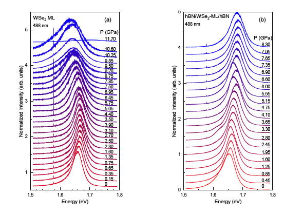
Figure 2: Normalized PL spectra measured at room temperature and as a function of pressure with 488-nm excitation (a) for the bare WSe2 ML and (b) for the hBN/WSe2-ML/hBN vdW heterostructure. The sharp line at 1.58 eV corresponds to the spurious signal from the 785 nm laser.
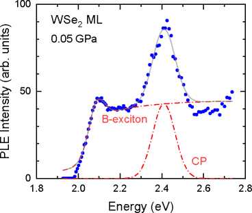
Figure 3: PLE spectrum (closed blue symbols) of the bare WSe2 ML at a very low pressure right after closing the DAC. The solid grey curve and the dash-dotted red curves represent the lineshape fitting function and its components, respectively, associated to the B-exciton and a critical point (CP).
Strikingly, the behavior of the A,B-excitons of the bare and encapsulated WSe2 ML is oppo-site. Whereas for the hBN/WSe2-ML/hBN het-erostructure both exciton energies increase linearly with increasing pressure with a coefficient of 3.53.8 meV/GPa, for the bare WSe2 ML the excitons decrease in energy with a slope of -3.1 and -1.3 meV/GPa for the A- and B-exciton, respectively. Comparing with the available literature data, the pressure coefficient of the A-exciton determined here for the encapsulated WSe2 ML is roughly one order of magnitude smaller than the one reported for a single ML of MoS2 (20 meV/GPa 14, 30 meV/GPa 15, 40 meV/GPa 16, 50 meV/GPa 17), WSe2 (32 meV/GPa 19) and WS2 (20 meV/GPa 20). All these data were obtained for monolayers on Si/SiO2 substrates, where the oxide layer was fairly thick, ranging between 200 and 300 nm. In the work of Han et al. 20, the same exper-iment is reported for a WS2 ML exfoliated directly onto the diamond and a much smaller pressure coef-ficient is found (10 meV/GPa). In the next section, we suggest a possible way to explain such a large disparity in the high pressure results concerning the excitonic properties of single MLs on the basis of a close inspection of the stress-strain relations.
ii. Stress-strain relations for different stress situations
First of all, we have to define the physical system for consideration of its stress/strain situation inside the DAC. It is a common practice to include the substrate supporting the 2D system, provided that adhesion forces between 2D sample and substrate are important. In this respect, we note that the conventional adhesion, corresponding to the ten-dency of two materials to cling to one another by van der Waals (vdW) forces is not relevant for high pressure experiments. The net vdW adhesion (at-tractive) force is perpendicular to the surfaces in contact and is proportional to the contact surface. Inside the diamond anvil cell (DAC), however, the substrate (or the diamond) will transmit the same pressure to the sample as it does the pressure trans-mitting medium, irrespective of the magnitude of the vdW adhesion force. This is just a requirement of the static equilibrium condition. In contrast, a "lateral" adhesion force acts solely in-plane, as is associated with the gliding of one object on a substrate. These lateral forces are typically much weaker than normal adhesion forces. An important exception for which lateral adhesion become signifi-cant concerns the case of a rough substrate surface (rippled) and a sample (a thin membrane) show-ing certain degree of conformation to the substrate surface (see Ref. 28). This can drive the trans-mission of in-plane strain (tensile or compressive) from the substrate to the sample, as pointed out by D. Machon et al. 29, being in principle relevant for high pressure experiments, mainly when sub-strate and sample exhibit different bulk modulus, i.e., different compressibility.
It has been shown 28 that a thin membrane characterized by a bending rigidity C would be conformal to a rippled surface with a curvature Kg and an adhesion energy (contact surface potential) 7, depending on the values adopted by a dimensionless parameter a = . Here Keq = is the equilibrium curvature of the membrane, which is determined by the ratio of the adhesion energy and the bending rigidity of the membrane. When a > 1 the membrane is expected to adhere well to the surface, whereas for a ^ 1 the membrane cannot adapt to the rippled surface and detaches from it being non-conformal. For the case of a 2D system with n layers, the bending rigidity depends on n, such that Cn increases sharply for an increasing number of layers. Thus, a is expected to decrease with increasing n. In fact, from the analysis of the Raman data regarding the in-plane strain transferred from a Si/SiO2 substrate to single, bilayer, and multi-layer graphene, it has been inferred that for n > 2 the 2D system looses its adhesion due to the enhanced rigidity of the multi-layers 29-31. Moreover, in the work of Alencar et al. 18 on the pressure behavior of MoS2 monolayers on Si/SiO2 substrates, it was argued that the unbinding of the transition metal dichalcogenide layer from the substrate can already occur for a single layer, because it has a much higher bending modulus than graphene 32. As a matter of fact, they observe a splitting of the Raman modes of the MoS2 ML, which is ascribed to the presence of regions with low and high conformation of the ML to the substrate, i.e. regions with different in-plane strain, affecting the frequency of the optical phonons. Concerning our case of having the 2D sys-tems directly transferred onto one on the diamond anvils, we can assume that the thick and much rigid hBN/WSe2-ML/hBN sandwich does not adhere to the diamond. In the case of the WSe2 monolayer, since we do not observe any splitting neither in the Raman modes (see discussion below) nor in the bright excitonic luminescence (PL), we can also as-sume that a situation of low conformation applies. Taking all the mentioned facts together, we are led to the conclusion that adhesion effects are not rel-evant for the proper interpretation of our experimental results and, hence, that we do not have to consider the diamond anvil as part of the physical system.
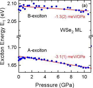
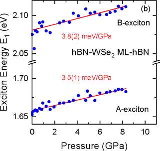
Figure 4: Ground state energy Ei of the A and B-exciton as a function of pressure (a) for the bare WSe2 ML and (b) for the hBN/WSe2-ML/hBN vdW heterostructure. Lines represent least-squares fits to the data points. Numbers in parentheses represent error bars.
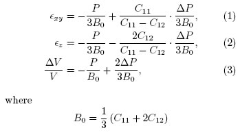
Let us consider that our 2D system corresponding either to the bare WSe2 ML or the hBN/WSe2-ML/hBN vdW heterostructure is well described just as a thin slab of thickness d inside the DAC, as sketched in Fig. 5. For a sufficiently thick slab, the stress situation would be hydrostatic (AP = 0). Our ansatz is that for vanishing thickness a depar-ture from the strictly hydrostatic situation would gradually develop. Below a certain critical value, the in-plane stress components will decrease with decreasing thickness by a certain amount AP. The reason is that for a vanishing slab cross section the molecules of the pressure medium are unable to transmit any momentum to the slab in the in-plane directions. In the limit of vanishing thickness d (a graphene ML, for example), the in-plane components of the stress tensor would also vanish (AP = P).
Although TMD monolayers belong to the D3h space group, from the point of view of their elas-tic properties it is a good approximation to use an elastic-stiffness tensor with cubic symmetry, i.e., C33 « C11 and C13 « C\2 33. Please, note that it is not correct to take the bulk values for C33, C13, because they are much smaller than for a ML due to inclusion of the weak vdW interlayer interac-tions. Under these assumptions (see also discussion in the Supplementary Material), we have derived the strain-tensor components e¿j and relative vol-ume change for the general stress situation of the slab in Fig. 5: where is the "bulk modulus" of the monolayer and the minus sign of the compressive pressure is explicitly written in the equations, such that 0 > AP > P. After Eqs. (1) to (3), the usual hydrostatic case corresponds to having AP = 0, for which all three strain tensor components are the same and com-pressive (exy = ez = - 3^-). This occurs for the several monolayers thick hBN/WSe2-ML/hBN het-erostructure. On the contrary, an effectively uniaxial stress situation sets in for AP = P. In this case, a compressive stress -P is applied from both sides and perpendicular to the plane of the slab, whereas the in-plane strain is tensile (e?)Tax' = - " Cl2 . eXy,dro-). We believe that this situation of highly, if not pure, uniaxial stress does apply for the bare WSe2 ML case, as we argue further below when discussing the Raman results. As a conse-quence, the sign of the linear pressure coefficient of the A and B-exciton energy changes from positive to negative for the bare ML as compared to the en-capsulated one because for the former the in-plane strain is tensile rather than compressive. Further-more, for all literature data, the stress situation corresponding to a ML on top of a SiÜ2/Si sub-strate is much more complicated. The bulk mod-ulus of the silicon oxide is about one third of that of Si. As discussed in detail in the Supplementary Material, a thick SiO2 layer epitaxially attached to Si will be strongly deformed when hydrostatic pressure is applied, due to the large biaxial tensile stress that the much thicker and less compressive Si exerts on the oxide layer, which under pressure tends to compress three times more than Si. As recognized in Ref. 20, the large deformation of the Si oxide layer introduces an extra strain of the TMD monolayer, which might be the reason for the observation of much higher pressure coefficients for the A,B-excitons.
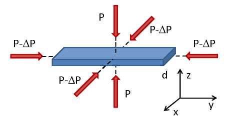
Figure 5: Schematic representation of the stress situation inside the DAC for a slab of thickness d. The stress tensor can depart from hydrostatic (AP = 0), if d ^ 0.
iii. Raman scattering under pressure
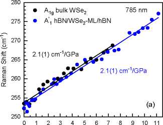
The dominant first-order Raman active modes of bulk 2H-WSe2 are the one with A1g symmetry, which involves atomic displacements in the direc-tion perpendicular to the layers, and the ones with E2g symmetry, for which the atomic displacements are in-plane 34. For a single monolayer, the corresponding Raman allowed modes with totally similar eigenvectors as for the bulk are the A'1 and E' modes. In WSe2 both mode types pos-sess very similar frequencies and in Raman spec-tra, both overlap with a very strong signal associated with second-order scattering processes in-volving two LA phonons (see representative Raman spectra in Figs. S4a-4d of the Supplementary Material). Nevertheless, the Raman signal of the A1g and A'i modes can be resonantly enhanced by tun-ing the laser wavelength to match the A-exciton energy E1 34,35. Near-resonance conditions are attained for bulk WSe2 and the ML with the red 633 nm laser line and the infrared (IR) 785 nm line, respectively. The reason for the resonant behavior is that in TMDs the A-exciton wavefunction con-tains a large weight from d?z orbitals of the metal atoms. This makes the A-exciton energy sensitive to movements of the metal atoms in the direction perpendicular to the layers, as is the case for the eigenvectors of the phonon modes with A symmetry. The non-resonant modes with E symmetry are better seen with blue excitation (488 nm) due to the 1/w4 prefactor in the Raman cross section. In the following, we show that by comparing the pressure coefficients of the Raman active modes obtained for the bulk and the encapsulated and bare monolayer, we are able to infer a different stress situation for the latter.
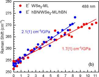
Figure 6a shows the results of the Raman mea-surements as a function of pressure for the modes with A symmetry measured with IR excitation for the hBN/WSe2-ML/hBN heterostructure and a piece of bulk WSe2 which was transferred onto the diamond together with the monolayer. Both slopes are within experimental uncertainty identi-cal, which speaks for a fully hydrostatic compres-sion of the encapsulated monolayer. In contrast, the pressure dependence of the Raman modes with E symmetry of the bare and encapsulated MLs is compared in Fig. 6b. Strikingly, the slope for the bare WSe2 ML is a factor 1.28 smaller than the one of the encapsulated ML. We note that for pure uniaxial compression of a cubic crystal like Si 36 a reduced pressure coefficient by roughly a factor 1.5 is expected for the Raman modes with displace-ments in the plane perpendicular to the stress. This is just a consequence of the tensile character of the in-plane strain when the material is uniaxially com-pressed in the perpendicular direction. We are thus led to the conclusion that for the bare ML the stress situation which is most likely established inside the DAC is almost purely uniaxial.
Pressure (GPa)
Pressure (GPa)
Figure 6: Comparison of the pressure dependence of first-order Raman active modes: (a) The A1g mode bulk WSe2 and the A'i of the hBN/WSe2-ML/hBN heterostructure measured with 785 nm excitation and (b) the E' mode of the bare WSe2 ML and hBN/WSe2-ML/hBN heterostructure. Lines represent least-squares fits to the data points and numbers in parentheses represent error bars.
IV. Conclusions
In summary, we have performed a comparative study of the pressure dependence of the optical transition energies corresponding to the radiative recombination of the A and B-excitons for a bare WSe2 ML and a hBN/WSe2-ML/hBN heterostructure, both transferred onto one of the diamonds of the DAC. We have found that for the encapsulated WSe2 ML the energy of both excitons increases with pressure with a relatively small slope of 3.5 to 3.8 meV/GPa, whereas for the bare ML both exci-tons decrease in energy. These results are at odds with available literature data which show much larger and positive pressure coefficients for a single WSe2 monolayer and other truly 2D TMD ma-terials. It is important to note that the literature data were almost exclusively obtained for monolay-ers deposited or transferred onto a thick SiO2 layer on top of a Si wafer. To explain the observed dis-crepancies between the different high pressure ex-periments on 2D TMDs, we have proposed a revi-sion of the stress situation in each particular case, which depends principally on the effective thick-ness of the slab being pressurized in the DAC. Here, we propose that for the bare single monolayer (case of vanishing thickness) the stress situa-tion is better described by using an uniaxial stress tensor, whereas for the much thicker hBN/WSe2-ML/hBN heterostructure conventional hydrostatic conditions can be assumed. Our Raman results, obtained simultaneously with the PL and PLE data in each case, speak in favor of such an interpretation. We believe that our findings will have significant impact on future high pressure work on truly 2D material systems like graphene, TMDs, BN, and other layered materials, for the assessment of the stress situation appears to be crucial for the cor-rect interpretation of the experimental results.
Acknowledgements - The Spanish Ministerio de Economía, Industria y Competitividad is grate-fully acknowledged for its support through Grant No. SEV-2015-0496 in the framework of the Span-ish Severo Ochoa Centre of Excellence program and Grant MAT2015-70850-P (HIBRI2). AFL ac-knowledges a FPI fellowship (BES-2016-076913) from the Spanish Ministerio co-financed by the European Social Fund and the PhD program in Materials Science from Universitat Autonoma de Barcelona in which he is enrolled.
1 A Splendiani, L Sun, Y Zhang, T Li, J Kim, C-Y Chim, G Galli, F Wang, Emerging photo-luminescence in monolayer M0S2, Nano Lett. 10, 1271 (2010). [ Links ]
2 K F Mak, C Lee, J Hone, J Shan, T F Heinz, Atomically thin MoS2: A new direct-gap semiconductor, Phys. Rev. Lett. 105, 136805 (2010). [ Links ]
3 G Wang, A Chernikov, M M Glazov, T F Heinz, X Marie, T Amand, B Urbaszek, Excitons in atomically thin transition metal dichalcogenides, Rev. Mod. Phys. 90, 021001 (2018). [ Links ]
4 D Xiao, G-B Liu, W Feng, X Xu, W Yao, Coupled spin and valley physics in monolayers of MoS2 and other group-VI dichalcogenides, Phys. Rev. Lett. 108, 196802 (2012). [ Links ]
5 G Wang, C Robert, M M Glazov, F Cadiz, E Courtade, T Amand, D Lagarde, T Taniguchi, K Watanabe, B Urbaszek, X Marie, In-plane propagation of light in transition meta! dichalcogenide monolayers: Optical selection rules, Phys. Rev. Lett. 119, 047401 (2017). [ Links ]
6 C Robert, T Amand, F Cadiz, D Lagarde, E Courtade, M Manca, T Taniguchi, K Watan-abe, B Urbaszek, X Marie, Fine structure and lifetime of dark excitons in transition meta! dichalcogenide monolayers, Phys. Rev. B 96, 155423 (2017). [ Links ]
7 M R Molas, C Faugeras, A O Slobodeniuk, K Nogajewski, M Bartos, D M Basko, M Potemski, Brightening of dark excitons in monolayers of semiconducting transition meta! dichalcogenides, 2D Mater. 4, 021003 (2017). [ Links ]
8 X-X Zhang, T Cao, Z Lu, Y-C Lin, F Zhang, Y Wang, Z Li, J C Hone, J A Robinson, D Smirnov, S G Louie, T F Heinz, Mag-netic brightening and control of dark excitons in monolayer WSe2, Nature Nanotechnol. 12, 883 (2017). [ Links ]
9 Y Zhou, G Scuri, D S Wild, A A High, A Dibos, L A Jauregui, C Shu, K De Greve, K Pistunova, A Y Joe, T Taniguchi, K Watanabe, P Kim, M D Lukin, H Park, Probing dark excitons in atomically thin semiconductors via near-field coupling to surface plasmon polari-tons, Nature Nanotechnol. 12, 856 (2017). [ Links ]
10 Z Jin, X Li, J T Mullen, K W Kim, Intrin-sic transport properties of electrons and holes in monolayer transition-metal dichalcogenides, Phys. Rev. B 90, 045422 (2014). [ Links ]
11 J Lindlau, C Robert, V Funk, J Forste, M Forg, L Colombier, A Neumann, E Courtade, S Shree, M Manca, T Taniguchi, K Watanabe, M M Glazov, X Marie, B Urbaszek, A Hogele, Identifying optical signatures of momentum-dark excitons in transition metal dichalco-genide monolayers, arXiv:1710.00988 (2017).
12 F Cadiz et al., Excitonic linewidth approach-ing the homogeneous limit in MoS2-based van der Waals heterostructures, Phys. Rev. X 7, 021026 (2017).
13 A R Goñi, K Syassen, Optical properties of semiconductors under pressure, Semicond. Semimetals 54, 247 (1998).
14 X Dou, K Ding, D Jiang, B Sun, Tuning and identification of interband transitions in monolayer and bilayer molybdenum disulfide using hydrostatic pressure, ACS Nano 8, 7458 (2014).
15 A P Nayak, T Pandey, D Voiry, J Liu, S T Moran, A Sharma, C Tan, C-H Chen, L-J Li, M Chhowalla, J-F Lin, A K Singh, D Akinwande, Pressure-dependent optical and vi-brational properties of monolayer molybdenum disulfide, Nano Lett. 15, 346 (2014).
16 F Li, Y Yan, B Han, L Li, X Huang, M Yao, Y Gong, X Jin, B Liu, C Zhu, Q Zhou, T Cui, Pressure confinement effect in MoS2 monolayers, Nanoscale 7, 9075 (2015).
17 L Fu, Y Wan, N Tang, Y Ding, J, Gao, J Yu, H Guan, K Zhang, W Wang, C Zhang, J-J Shi, X Wu, S-F Shi, W Ge, L Dai, B Shen, K-A crossover transition in the conduction band of monolayer MoS2 under hydrostatic pressure, Sci. Adv. 3, e1700162 (2017).
18 R S Alencar, K D A Saboia, D Machon, G Montagnac, V Meunier, O P Ferreira, A San-Miguel, A G Souza Fihlo, Atomic-layer MoS2 on SiO2 under high pressure: Bimodal ad- hesion and biaxial strain effects, Phys. Rev. Mater. 1, 024002 (2017).
19 Y Ye, X Dou, K Ding, D Jiang, F Yang, B Sun, Pressure-induced K-A crossing in monolayer WSe2, Nanoscale 8, 10843 (2016).
20 B Han, F Li, L Li, X Huang, Y Gong, X Fu, H Gao, Q Zhou, T Cui, Correlatively depen-dent lattice and electronic structural evolutions in compressed monolayer tungsten disulfide, J. Phys. Chem. Lett. 8, 941 (2017).
21 T Taniguchi, K Watanabe, Synthesis of high-purity boron nitride single crystals under high pressure by using BaBN solvent, J. Cryst. Growth 303, 525 (2007).
22 H-K Mao, J Xu, P M Bell, Calibration of the ruby pressure ga,uge to 800 kbar under quasi-hydrostatic conditions, J. Geophys. Res. 91, 4673 (1986).
23 A Carvalho, R M Ribeiro, A H Castro Neto, Band nesting and the optical response of two-dimensional semiconducting transition metal dichalcogenides, Phys. Rev. B 88, 115205 (2013).
24 M. Wojdyr, Fityk: A general-purpose peak fit-ting program, J. Appl. Cryst. 43, 1126 (2010).
25 M Brotons-Gisbert, A Segura, R Robles, E Canadell, P Ordejon, J F Sánchez-Royo, Optical and electronic properties of 2H-MoS2 under pressure: Revealing the spin-polarized nature of bulk electronic bands, Phys. Rev. Mater. 2, 054602 (2018).
26 A R Goñi, A Cantarero, K Syassen, M Cardona, Effect of pressure on the low-temperature excitonic absorption in GaAs, Phys. Rev. B 41, 10111 (1990).
27 A R Goñi, K Syassen, M Cardona, Direct band gap absorption in Germanium under pressure, Phys. Rev. B 39, 12921 (1989).
28 O Pierre-Louis, Adhesion of membranes and filaments on rippled surfaces, Phys. Rev. E 78, 021603 (2008).
29 D Machon, C Bousige, R Alencar, A Torres-Dias, F Balima, J Nicolle, G S Pinheiro, A G Souza Filho, A San-Miguel, Raman scatter-ing studies of graphene under high pressure, J. Raman Spectrosc. 49, 121 (2018).
30 C Bousige, F Balima, D Machon, G S Pin-heiro, A Torres-Dias, J Nicolle, D Kalita, N Bendiab, L Marty, V Bouchiat, G Montagnac, A G Souza Fihlo, P Poncharal, A San-Miguel, Biaxial strain transfer in supported graphene, Nano Lett. 17, 21 (2017).
31 J Nicolle, D Machon, P Poncharal, O Pierre-Louis, A San-Miguel, Pressure-mediated dop-ing in graphene, Nano Lett. 11, 3564 (2011).
32 J-W Jiang, Z Qi, H S Park, T Rabczuk, Elas-tic bending modulus of single-layer molybde-num disulfide (MoS2): Finite thickness effect, Nanotechnol. 24, 435705 (2013).
33 L-P Feng, N Li, M-H Yang, Z-T Liu, Effect of pressure on elastic, mechanical and electronic properties of WS&¿: A first-principles study, Mater. Res. Bull. 50, 503 (2014).
34 S V Bhatt, M P Deshpande, V Sathe, R Raoc, S H Chakia, Raman spectroscopic investiga-tions on transition-metal dichalcogenides MX2 (M =Mo, W; X = S, Se) at high pressures and low temperature, J. Raman Spectrosc. 45, 971 (2014).
35 T Livneh, J S Reparaz, A R Goñi, Low-temperature resonant Raman asymmetry in 2H-MoS2 under high pressure, J. Phys.: Con-dens. Matter 29, 435702 (2017).
36 E Anastassakis, M Cardona, Phonons, strains, and pressure in semiconductors, Semicond. Semimetals 55, 117 (1998).

